- Home
- Prelims
- Mains
- Current Affairs
- Study Materials
- Test Series
GPU chips and Semiconductor Geopolitics
- In December 2025, a landmark shift in U.S. technology policy allowed Nvidia to resume selling its high-end H200 GPU chips to "vetted" Chinese buyers. This decision by the Trump administration marks a transition from a "containment" strategy to a "transactional" one, with profound geopolitical implications for the global AI race, domestic industry, and international alliances.
- The Strategy of "Enforced Dependency"
- The central geopolitical gamble is that by providing China with advanced—but not cutting-edge—U.S. chips, the U.S. can slow China’s pursuit of technological self-reliance.
- Starving Local Competitors: U.S. officials and Nvidia CEO Jensen Huang argue that if Chinese tech giants like Alibaba, ByteDance, and Tencent can buy superior Nvidia hardware, they will have less incentive to invest billions in local alternatives like Huawei’s Ascend line.
- The Technology Gap: The H200 is significantly more powerful than the previously permitted H20 chip (roughly six times more capable), yet it remains a generation behind Nvidia’s flagship Blackwell and upcoming Rubin architectures. By keeping the most advanced chips restricted, the U.S. seeks to maintain a permanent 18-to-24-month lead in AI capabilities.
- Transactional Diplomacy: The "Rare Earths" Exchange
- The deal is not merely about semiconductors; it is part of a broader "trade truce" and strategic resource swap.
- Rare Earth Access: In exchange for loosening chip curbs, the U.S. secured a commitment from Beijing to lift its own export controls on critical minerals like gallium, germanium, antimony, and graphite. These are essential for U.S. defense manufacturing and high-tech industries where China currently holds a near-monopoly.
- The 25% "Transaction Fee": In a move described as a hallmark of his administration''s transactional approach, President Trump mandated that the U.S. government receive a 25% fee on the revenue from every Nvidia chip sold to China. This effectively turns national security policy into a significant source of federal revenue.
- Impact on the Global AI Arms Race
- The resumption of sales has immediate consequences for the "AI arms race" between the two superpowers:
- Military Parity Risks: Critics argue that the H200 is powerful enough to drive sophisticated military applications, including autonomous drone swarms and battlefield targeting algorithms.
- Algorithmic Efficiency: Before the ban was lifted, Chinese firms like DeepSeek demonstrated they could achieve breakthroughs even with restricted hardware. The availability of H200-level compute power is expected to drastically accelerate their development timelines for next-generation Large Language Models (LLMs).

- Geopolitical Friction with Allies
- The sudden policy reversal has created tension with U.S. allies in the Netherlands (ASML) and Japan, who were pressured to restrict their own exports to China under the previous U.S. regime.
- Trust and Consistency: Allies now face a "hard choice" as they see the U.S. prioritizing its own commercial interests and revenue over the collective security framework they were asked to support.
- A "Turnstile" for Technology: Security analysts warn that this deal transforms the "high fence" around sensitive technologies into a "turnstile" that can be opened for the right price, potentially undermining future international cooperation on technology controls.
Comparison of Key Chips in the Deal
| Chip Model | Status in China (Dec 2025) | Performance Context |
| Nvidia H20 | Previously allowed; now being phased out. | Redesigned for China; roughly 700x less powerful than the flagship H100. |
| Nvidia H200 | Newly Approved for vetted buyers. | Roughly 6x more powerful than the H20; supports massive AI training. |
| Nvidia Blackwell | Strictly Banned. | Current cutting-edge architecture; restricted to U.S. and allied markets. |
What is Semiconductor Chip in GPU ?
- A semiconductor chip in a GPU (Graphics Processing Unit) is a tiny complex integrated circuit (IC) or microchip made from a single piece of silicon with billions of transistors, acting as the brain for rendering visuals and performing massive parallel computations, essentially an integrated circuit designed for complex, simultaneous calculations, making it crucial for gaming, AI, and video processing by handling tasks in parallel unlike a CPU.
- Transistors serving as the building blocks of semiconductor chips fabricated on wafers using specific technologies, enabling the creation of complex devices powering modern technology.
| Semiconductor: Semiconductors possess electrical conductivity properties intermediate between conductors and insulators, which can be modified by introducing dopants. |

Semiconductor Chips:
- It is a tiny electronic device made of semiconductor material (usually silicon or germanium) which serves as the basic building block of most electronic circuits.
- These chips can contain billions of microscopic switches on a chip smaller than a fingernail.
- The basic component of a semiconductor chip is a silicon wafer etched with tiny transistors that control the flow of electricity according to various computational instructions.
- It performs various functions, such as processing data, storing information, or controlling electronic devices.
- They are a critical part of almost every modern electronic device, including smartphones, computers, and integrated circuits.
Transistor:
- Transistors are fundamental components of semiconductor devices that amplify or switch electronic signals and electrical power.
- They are the building blocks of modern electronic devices and are used in various applications, including amplifiers, switches, and digital circuits.
Fabrication Technology
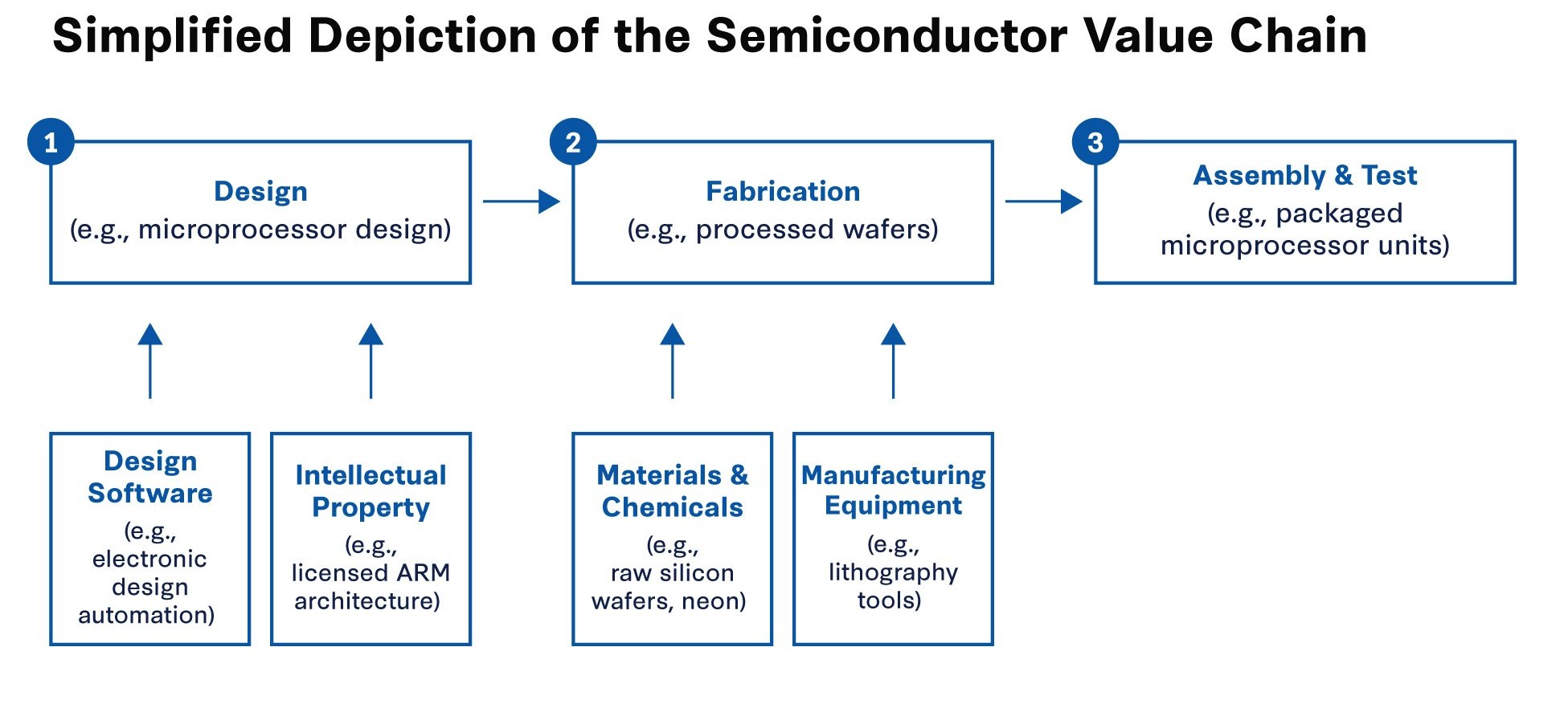
- Fabrication technology refers to the process of creating semiconductor devices like chips and transistors. It involves several key steps, including wafer preparation, photolithography, etching, doping, and packaging.
Wafer:
- A wafer (also called a slice or substrate) is a thin slice of semiconductor material, such as crystalline silicon, used for the fabrication of integrated circuits.
- A semiconductor chip is produced by printing an array of chips on a circular semiconductor wafer, similar to how postage stamps are printed on a sheet and then cut out individually.
- Larger wafer sizes in the industry enable more chips to be printed on a single wafer, accelerating and reducing the cost of chip production, despite the technical challenges and initial capital expenses involved.
What is the Status of India’s Semiconductor Ecosystem?
- India is actively pursuing the development of a robust semiconductor ecosystem. With its large market potential, talent pool, and government support. India aims to reduce dependence on imports and establish domestic manufacturing capabilities.
- India''s established chip design industry since the 1990s will aid its semiconductor manufacturing efforts, offering opportunities for various professionals beyond electronics and computer engineers.
- The Government of India has implemented several strategic initiatives through the India Semiconductor Mission (ISM), supported by a total outlay of ₹76,000 crore. These programs aim to build a self-reliant ecosystem covering design, fabrication, and testing.
- India Semiconductor Mission (ISM) Schemes
The ISM serves as the nodal agency for implementing four major fiscal support schemes:
- Semiconductor Fabs Scheme: Provides 50% fiscal support on a pari-passu basis for setting up Silicon CMOS-based wafer fabrication plants in India.
- Display Fabs Scheme: Offers 50% financial assistance for the project cost of setting up display fabrication units (e.g., AMOLED and LCD).
- Compound Semiconductors and ATMP/OSAT Scheme: Extends 50% fiscal support on capital expenditure for compound semiconductor fabs, sensors, and Outsourced Semiconductor Assembly and Test (OSAT) facilities.
- Design Linked Incentive (DLI) Scheme: Supports domestic startups and MSMEs with incentives up to ₹15 crore for product design and 6%–4% of net sales over five years as a deployment incentive.
- Manufacturing & Infrastructure Support
- Production Linked Incentive (PLI): Incentivizes domestic manufacturing of large-scale electronics and IT hardware, offering 3% to 6% on incremental sales.
- Scheme for Promotion of Manufacturing of Electronic Components and Semiconductors (SPECS): Provides a 25% financial incentive on capital expenditure for manufacturing electronic components and semiconductors.
- Modernization of Semi-Conductor Laboratory (SCL): The government approved the modernization of the SCL in Mohali as a brownfield fab to improve efficiency and cycle time.
- Electronics Manufacturing Clusters (EMC 2.0): Offers financial assistance (up to 50% of project cost) to develop shared infrastructure and common facilities for electronics manufacturers.
- Talent and Workforce Development
To meet the projected requirement of one million skilled workers by 2030, the government has launched several talent-focused programs:
- Chips to Startup (C2S) Programme: Aimed at training 85,000 engineers at over 113 academic institutions in VLSI and embedded system design.
- AICTE New Curriculum: Introduced specialized B.Tech, Diploma, and Minor degrees in VLSI Design & Technology and IC Manufacturing.
- SMART Lab: Established at NIELIT Calicut with a target to train one lakh engineers nationwide.
- Industry Collaborations: MoUs signed with global leaders like Lam Research (to train 60,000 engineers via the Semiverse platform), IBM, and Purdue University for R&D and skill building.
- Major Approved Projects (2025 Status)
By late 2025, 10 units have been approved under the Semicon India program with a cumulative investment of approximately ₹1.6 lakh crore.
- Tata-PSMC Fab: India''s first commercial silicon fab in Dholera, Gujarat.
- Micron Technology: A major ATMP facility in Sanand, Gujarat, expected to roll out "Made in India" chips by late 2025.
- Tata Semiconductor Assembly and Test (TSAT): A large-scale facility in Morigaon, Assam.
- CG Power-Renesas: An OSAT facility in Sanand, Gujarat, featuring an end-to-end pilot line.
- HCL-Foxconn JV: Approved to manufacture display driver chips in Uttar Pradesh.
Key Advantages
- Market Potential: India’s rapidly growing population and burgeoning middle class create a strong demand for semiconductor products.
- India’s semiconductor market is projected to reach $55 billion by 2026, reflecting its focus on domestic manufacturing.
- Talent Pool: India emphasises skill development and innovation, encouraging domestic chip design skills.
Conclusion
- In 2025, the geopolitics of semiconductors and GPUs have reached a transformative conclusion: computing power is now the definitive metric of national sovereignty. The shift from a policy of pure denial to one of "transactional dependency"—exemplified by the Nvidia H200 sales to China—signals that the U.S. and its allies are now prioritizing long-term economic leverage and software ecosystem dominance over immediate hardware containment.As 2026 approaches, the "Silicon Curtain" is no longer a solid wall, but a monetized filter designed to extract maximum economic value for the U.S. while attempting to manage China''s rise through controlled technological dependency.


 Latest News
 General Studies